
Tackling Complex Challenges in Semiconductor Chiplet Testing
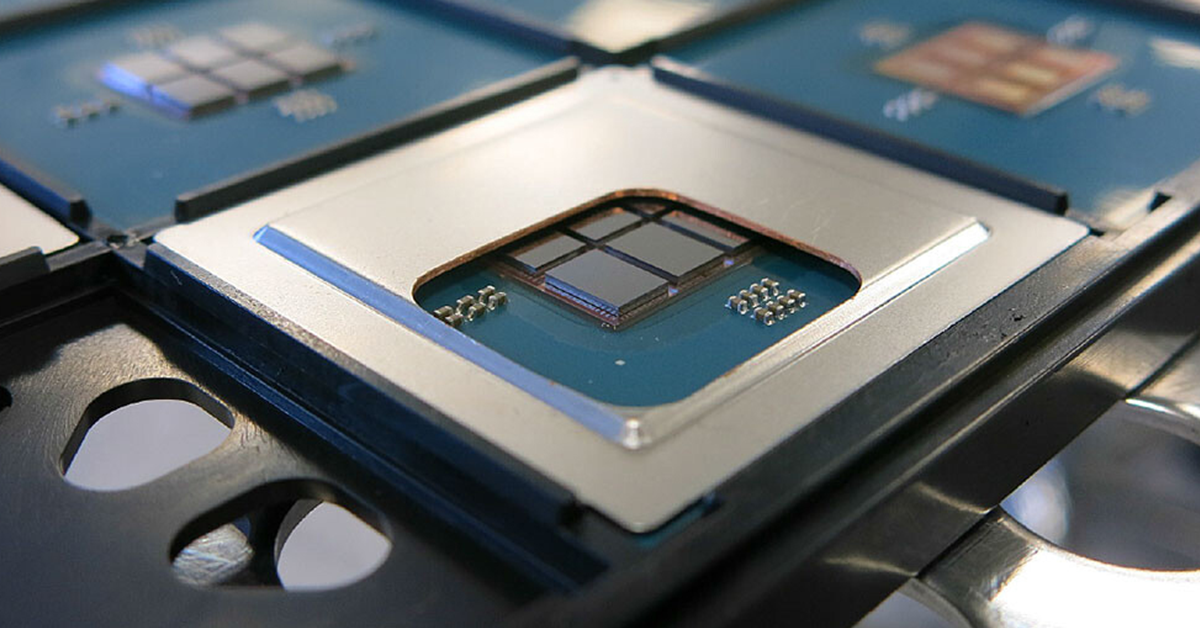
In semiconductor technology, chiplets have emerged as modular components that can operate either independently or collectively on a single substrate. Unlike monolithic chips that manage all functions in one unit, chiplets streamline design by allocating specific tasks to separate ICs. This modular design not only offers flexibility, optimized performance and efficiency, but also presents unique challenges when it comes to testing and validation, as we’ll explore in this article.
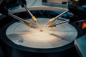
Testing chiplets presents a challenging task due to their increasing complexity, often denser process technology, and the push for higher performance. Probers are used to test chiplets before they are co-packaged into a complete solution. The densely populated chiplets, with their complex interconnects, make it a difficult task for a prober to fully assess the functionality and performance of a chiplet. A lack of comprehensive testing at the probing stage means that yield fallout at the final test will be costly. Other challenges include managing large volumes of test data, navigating complex interface protocols, and meeting high-speed requirements. However, addressing these challenges is crucial for ensuring the functionality and performance of modern semiconductors.
Testing Chiplets with Automated Test Equipment
Automated Test Equipment (ATE) systems are connected to a prober to verify that an integrated circuit is ready for packaging. Typically, the packaged IC is tested again at the final test on ATE alone to validate the device more comprehensively and at speed. This combination of an ATE system and a prober is also used to test chiplets that will be combined on a single substrate and assembled to resemble a single packaged IC. While the process for single-chip probing and multi-chip probing appears the same, the requirements of multi-chip probing are more stringent for economic reasons. For example, probing a single die that results in a 90% final test yield might be sufficient, but the total yield for a 3-chiplet module (with each module yielding 90%) would be only 73%. While a probe escape in a single chip results in discarding a good package and a bad die, in the module configuration, you would discard an expensive good package and likely two good dies along with the bad one. In addition, this leads to increased overall test costs due to the lower final test yield. This underscores the critical importance of comprehensively probing chiplets.
Some of the challenges of testing semiconductors to be used as chiplets at probe can include:
- Known Good Die: Traditionally, probing has been used to screen failures, thereby avoiding large yield fallout at package test on ATE. The ATE provides a more suitable environment for complete verification, ensuring that the final test catches anything not detected during probing. Chiplets need to be thoroughly verified in die form to prevent yield fallout once they are combined with other chiplets in a complete package. This means that the bar for testing at the probing stage is much higher than for single die packaged parts.
- Signal Integrity: As chiplets are designed to drive signals over short distances during normal usage, their I/Os are optimized for power efficiency, resulting in relatively weak outputs. When probing a chiplet, the outputs are required to drive the line back to the tester, a demand that exceeds the buffer’s capability. This limitation significantly slows down the test time and eliminates the possibility of testing at speed.
- Complex Interconnects: Many chiplets function as protocol translators, enabling the final packaged product to communicate with multiple interfaces. These complex protocols must be thoroughly verified at the die level. This necessitates at-speed testing in an environment with signal loss.
- Complex Designs: Chiplets frequently employ low geometry FinFet technology, leading to incredibly complex designs. Thoroughly testing these designs becomes a slower and more challenging process. This complexity can be compounded by the need to slow down I/Os to accommodate signal integrity and interconnect issues.
- Throughput: The complexity of chiplets and their interconnect challenges present significant obstacles to rapid testing. Ideally, multiple dies would be probed in parallel to enhance efficiency. However, the increased number of I/Os in chiplets requires an even greater number of tester I/Os, complicating the parallel testing process.
Addressing chiplet testing challenges with a prober and ATE system requires expertise in semiconductor testing, proper equipment selection, and meticulous testing procedures. Effective solutions often demand collaboration among chip designers, test engineers, and equipment manufacturers.
A New Alternative Emerges to Chiplet-Based Semiconductor Testing
Elevate is pioneering new strategies in chiplet-based semiconductor testing. They’re exploring the shift of specific semiconductors from the traditional Automated Test Equipment (ATE) tester to the probe card, which could offer numerous testing advantages including:
- Improved Signal Integrity & Optimized Signal Routing: The proximity of Pin Electronics and DPSs to the DUT allows for shorter, less lossy, and less complex signal routes, resulting in better signal integrity at the DUT. This improvement in high-speed signal integrity enables at-speed testing, which can lead to more comprehensive testing and higher yield at final test. Additionally, shorter paths from the DPS to the DUT facilitate reduced supply droop, eliminating false errors and improving overall test repeatability.
- Reduced Tester Complexity: While the complexity of the probe card increases, the complexity of the tester decreases. Developers can optimize the probe card for the specific chiplet being tested, resulting in improved performance and faster test times, while also reducing capital expenditure as complex testers become unnecessary. Additionally, since signals originate from the probe card, ‘copy exact’ requirements can be maintained across multiple testers and configurations.
- Shorter Test Times: Placing more PE and DUT pins on the probe card enables significantly more parallel testing, effectively reducing test times.
Parallel Testing: Ideally, probing should occur as close to a single touchdown as possible. By eliminating connector constraints, the extent to which parallelism can be employed increases tremendously, thereby significantly enhancing testing efficiency.
Scalability: Once developed, probe card test solutions can be leveraged to test similar chiplets at lower development cost. - Customization: Prober-based testing solutions can be customized to meet the specific requirements of different chiplet designs, ensuring precise and tailored testing for each chiplet configuration.
- Lower Contact Resistance: Although contact resistance remains consistent across different probe solutions, the availability of additional sense pins facilitates remote and Kelvin sensing. This capability is useful for calibration or for compensating for contact resistance.
- Flexibility: Prober-based testing systems can be adapted for various chiplet configurations, making them suitable for testing different chiplet designs.
- Compatibility: With more functional and performance parameters handled at the probe card, the interface to the tester becomes less stringent. This allows copy exact waveforms to be present at the DUT regardless of the tester platform selected.
Join Elevate Semiconductor in Pioneering the Future of Chiplet Testing Through Innovative Collaborations.
Elevate Semiconductor is pioneering advancements in semiconductor testing by integrating our ATE semiconductors with prober cards. This innovation promises improved signal integrity, faster testing, and tailored solutions for diverse chiplet designs. We’re actively seeking partnerships with ATE and prober manufacturers to reshape the future of chiplet testing and contribute to the continued evolution of semiconductor testing technologies.