
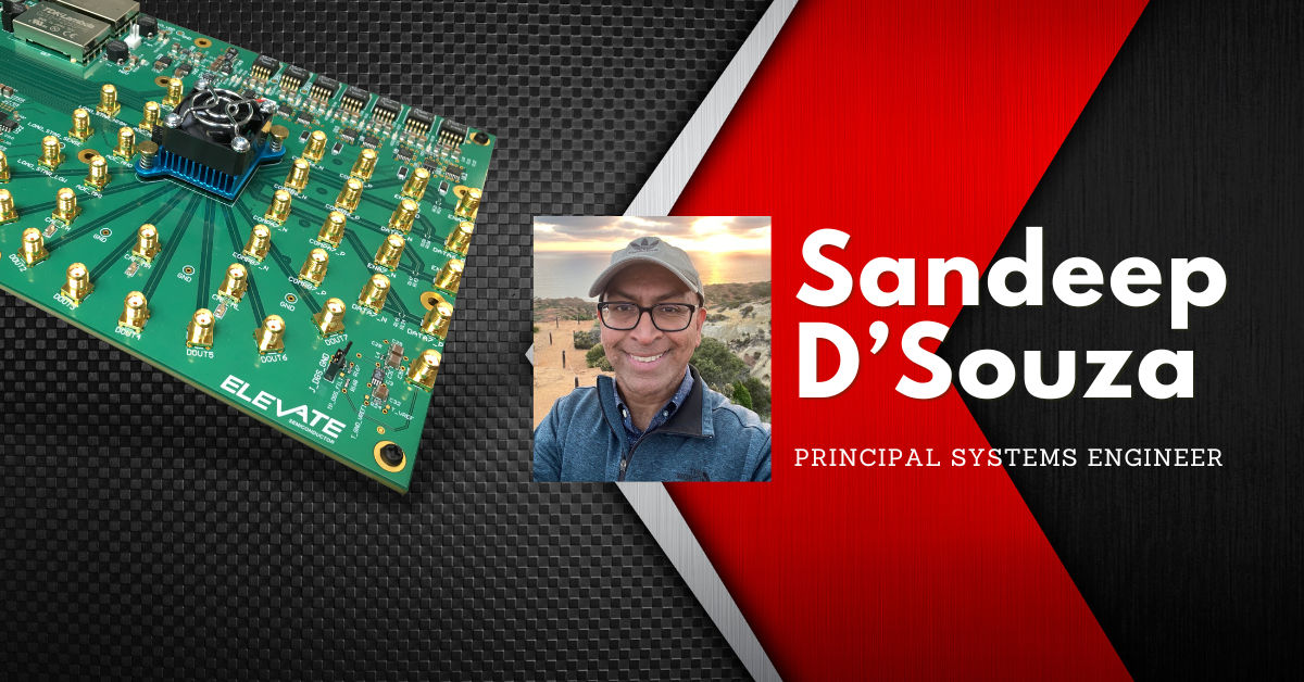
Interview with Dr. Sandeep D’Souza: A Visionary in Semiconductor Engineering
Interviewer: Welcome, Sandeep! Thank you for joining us today. Let’s start by getting to know you better. Could you introduce yourself and share some of your hobbies and interests?
Sandeep D’Souza: Thank you for having me. My name is Sandeep D’Souza, and I’m an electrical engineer based in San Diego, where I’ve lived for the past 11 years. Outside of my professional life, I’m passionate about travel, exploring new cuisines, and hiking. I also cherish the time spent doing volunteer community service alongside my wife and son. It’s a wonderful way to connect with the community and make a meaningful contribution.
Interviewer: That sounds incredibly rewarding. Now, turning to your professional journey, could you outline your extensive experience in the semiconductor industry?
Sandeep D’Souza: Certainly. I’ve been involved in the semiconductor industry since 1997. My academic background includes a PhD from UCLA, a Masters from Purdue University, and a Bachelor’s degree from the Indian Institute of Technology in Bombay, all in Electrical Engineering. Throughout my career, I’ve authored eight publications and am an inventor on over forty issued or pending patents.
Most recently, I was with Qualcomm in San Diego until last December, working as a Principal Systems Engineer. There, I contributed to several pioneering projects, including the industry’s first ultrasonic fingerprint sensor, which has been integrated into over 150 million devices worldwide, as well as developments in Smart-Haptics and other multimedia R&D technologies for mobile devices.
Before Qualcomm, from 2011 to 2013, I was a Principal Mixed-Signal IC Design Engineer at Semtech Corporation in Redondo Beach. My work focused on ultra-high-speed Analog-to-Digital and Digital-to-Analog data converters for use in coherent optical transceivers and digital microwave transceivers.
Even earlier, from 2009 to 2011, I was engaged as a PhD researcher at UCLA under Professor Frank Chang in the High-Speed Electronics Laboratory. There, I designed a 10-bit, 2 GSample/second DAC for a Self-Healing 60GHz Wireless Transceiver.
Prior to my time at UCLA, I worked as an RFIC designer at Skyworks Solutions in Irvine, CA, from 2006 to 2009, where I was involved in developing the industry’s first single-chip, multi-band WCDMA/EDGE/GSM Cellular transceiver. My career began at Conexant Systems in Newport Beach, CA, where I served as an Analog/Mixed-Signal/RF semiconductor device modeling engineer from 1997 to 2005.
Interviewer: Sandeep, what inspired your move to ElevATE and what can you tell us about the role you play there?
Sandeep D’Souza: My decision to join ElevATE was primarily influenced by the crucial role that Automated Test Equipment (ATE) plays within the semiconductor industry. ATE is vital for ensuring that integrated circuits deliver on their promised feature sets, performance, and reliability. It’s often perceived that the value of an integrated circuit is determined solely by its design. However, a deeper understanding reveals that its real test comes during the evaluation phase—essentially, a chip is only as good as it is tested.
At ElevATE, we work on chips that test other industry-leading chips, which means our products need to perform at even higher levels. Our devices must be more precise, faster, and capable of operating over wider voltage and current ranges compared to the high-quality devices we test.
Furthermore, the environment at ElevATE is fostered by a supportive and nurturing small-company atmosphere created by our executive management. This setting enables our team, who all possess deep technical expertise, to truly make a significant impact and bring out their best abilities.
Interviewer: Can you describe your current role and the projects you are focusing on?
Sandeep D’Souza: Certainly. I currently hold the position of Principal Systems Engineer within the design team, under the supervision of our VP of Engineering, Simon Leigh. My main project at the moment is the Whitney two-channel, high-voltage, highly-integrated System-on-a-Chip (SOC) Parametric Measurement Unit (PMU). This SOC is capable of performing multiple functions essential for testing semiconductor devices. Each channel in the Whitney can force voltage, force current, measure voltage, measure current, and make window compare measurements, utilizing six 16-bit DACs to achieve these capabilities. The functionality of the Whitney is managed through an SPI interface capable of clocking up to 50MHz.
In addition to the Whitney project, I am also involved in defining the roadmap for our next-generation PMUs. These include general-purpose PMUs for ATE, as well as specific PMU architectures targeting ATE for Battery Management Systems (BMS) in electric vehicles (EVs) and stationary battery energy storage systems (BESS). These projects are crucial for advancing our capabilities in semiconductor testing, catering to evolving market needs.