Typical integrated circuit (IC) solutions for pin electronics (PE) have been provided by multiple semiconductor companies in multiple different process technologies. Over the years, a typical chipset in support of all the functionality for a single device-under-test (DUT) has included bipolar, complementary bipolar, BiCMOS, SiGe BICMOS, CMOS, HV CMOS, and GaAs, as well as field programmable gate arrays (FPGAs). Each of these different technologies used for a different ATE function is packaged separately. This has led to solutions for ATE that take up a significant amount of board space, as well as a significant amount of power dissipation and cost, and the difficulties of dealing with the associated heat removal for the thermal design of a channel. This has produced limitations in the board size of a channel and limited the number of devices that can be tested in parallel, which impacts the $ / device test time. This has also been a cost and power problem. New advanced CMOS technologies provides a paradigm shift in ATE. CMOS can provide high levels of integration, large numbers of channels on a single die, and lower power and cost. The ability to integrate in CMOS will also enable the ability to test multiple devices in parallel, thus reducing test time and test cost per DUT. This trend has been initiated by new unique process features for CMOS which enables this new type of ATE. Smaller channel size, lower cost and power, and multiple DUTs tested in parallel are concepts that previously without taking advantage of the CMOS process technology evolution. Today you can fit 64 high speed digital channels on PXI instrument card and 192+ channels on a typical instrument card. This level of channel density enables testing of as many as 32, 64 or hundreds of DUT’s in parallel.
Silicon bipolar technology has been used historically for ATE pin electronics integrated circuits. This was the result of the fact that large voltage swings for the pins are needed, and the breakdown voltage of the bipolar transistor in older bipolar technologies could support these requirements. In recent years, silicon germanium (SiGe) BiCMOS technologies has also been considered for PE. There are multiple bipolar device types in SiGe technologies which allow the trade-off between breakdown voltage and device FT. Additionally, the emitter feature sizes for the SiGe bipolar device allow for more than one PE channel to be integrated onto the same die as well as some CMOS support circuitry for the controls for the pin electronics. This is the result of being able to take advantage of CMOS devices in SiGe BiCMOS technologies with channels lengths of 0.35 mm down to 0.18 mm.


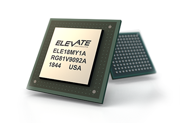
Mystery: SOC Octal 500 MHz Integrated Pin Electronics
Currently, bipolar is still a consideration for pin electronics in support of board level products, for markets such as automotive, but for testing of current and future SOCs, for a number of new and emerging high volume markets, using advanced ATE, where the cost per channel ($ / channel) has become an issue for these new test platforms, CMOS has become a competitor for bipolar for a number of reasons. The current and future drive for ATE electronics is to reduce the $ / channel, as well as the physical board size per channel in the ATE, and this is a difficult proposition with either bipolar or SiGe BiCMOS. Analog mixed signal CMOS technology nodes continue to be driven downwards, along with associated breakdown voltages, but the addition of some specialty devices to these technologies, such as variable drain devices, which enable analog mixed signal CMOS devices with high breakdown voltages (HV), allow the possibility of the inclusion of pin electronics in analog mixed signal CMOS. Current HV devices support > 30V breakdown, and this will evolve to > 50V. Current PE CMOS solutions are migrating from 180 nm to 65 nm, and the HV device capability is increasing with this technology node reduction.
The ATE support electronics are becoming SOCs themselves, with the integration of many functions that used to be separate packaged devices in specialty processes, such as timing generation, are now being able to be included in CMOS processes with high levels of integration. The ability to integrate analog and digital ATE functions into a single SOC provides the opportunity to reduce the size and cost of the ATE. Additionally, all of the signal processing and digital calibration can be included on-chip which will make the devices easier to deploy. ATE customers that currently have timing generators (TG) implemented in FPGAs now have the opportunity to include this functionality in a custom SOC that includes the PE. This integration opportunity provides the ability to have customer-specific TG IP on the same SOC as the PE. The TG will be higher resolution, lower jitter, and have more programmability and flexibility for the customer than the current FPGA solutions. Taking advantage of CMOS node scaling, this also leads to lower $ / channel, lower power, and a smaller footprint on the board.
This push towards the reduction of board size for ATEs is also enabled by the consideration of utilizing the HV CMOS devices to replace functions that have been classically discrete devices on the boards. These CMOS HV devices also have multiple gates, which can be taken advantage of through known design techniques to support large voltage swings. The HV device also enables the integration of ATE functions such as the parametric measurement unit (PMU) and the device power supply (DPS) on the same SOC as the PE and the TG and support many channels on a single die. Thus, analog mixed signal CMOS technology is driving towards reduction of channel size and cost through the integration of multiple device types that have historically been discrete surface mount (SMT) devices and separate packaged devices in different process technologies. As the frequency performance of the HV CMOS devices continue to increase, there will be more opportunities for CMOS to rival and replace bipolar and SiGe technologies for functions in the ATE that have been historically bipolar. Currently HV CMOS can support > 200-400 MBps pin electronics. This will evolve to 2-4 GBps with analog mixed signal CMOS process evolution, with the numbers of PE channels exceeding 8. Board size per channel is a critical consideration. All functions that can be integrated through the leverage of the HV CMOS and the smaller geometry CMOS devices can take advantage of this technology to do. This will ideally result in a board with large valued capacitors and CMOS SOCs, and this shrinks the board size to the ultimate physical limits possible.
In terms of improving channel density, analog mixed signal CMOS has provided an increase in channel density from 2 channels per chip to most commonly 8 channels per chip with the per channel power dissipation dropping by 2X to 4X lower than comparable bipolar products. The reduction in CMOS technology nodes will enable smaller packaging, lower power dissipation, higher levels of integration, and lower cost. All of these factors will contribute to a reduction in the $ / channel that CMOS will provide that bipolar will not be able to compete with. Additionally, current CMOS designs can be ported to lower nodes at a reduction in development costs as well as production cost. The utilization of advanced analog mixed signal CMOS can be used to develop SOC solutions for ATE customers that will provide a reduction in $ / channel cost for the final ATE product. The future of ATE is testing SOCs with higher pin counts and higher speeds, as the CMOS technology nodes continue to shrink. In order to meet these challenges, ATE chip solutions are needed that keep pace. It is an obvious natural progression for the PE and supporting ATE functions to shrink as well to keep up. There is the opportunity to realize this trend and continue down this path to provide unique ATE solutions that provide high speed ATE solutions at lower power, while reducing $ / channel and accompanying board space. Unique ATE SOC solutions can provided based on this realization to your company and allow you to provide a solution that is a discriminator in the ATE marketplace.


